SPI to AXI4-Lite Bridge
An SPI to AXI4-lite bridge for accessing AXI4-lite register banks, such as the ones generated by airhdl.com, over a serial peripheral interface (SPI).
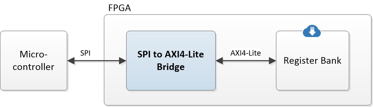
Using the Core
The SPI to AXI4-lite bridge comes as single, self-contained file for easy integration into your design. It is available in both VHDL and SystemVerilog versions:
- VHDL version:
/src/spi2axi.vhd
- SystemVerilog version:
/src/spi2axi.sv
SPI Modes
The SPI to AXI4-Lite bridge supports all four SPI modes, as defined in the following table:
| Mode |
Clock polarity (CPOL) |
Clock Phase (CPHA) |
Description |
| 0 |
0 |
0 |
Idle clock level is 0, data captured on leading (rising) clock edge. |
| 1 |
0 |
1 |
Idle clock level is 0, data captured on trailing (falling) clock edge |
| 2 |
1 |
0 |
Idle clock level is 1, data captured on leading (falling) clock edge. |
| 3 |
1 |
1 |
Idle clock level is 0, data captured on leading (falling) clock edge. |
Notes:
- All SPI bytes are transferred MSB-first.
- The SPI mode is configured statically using the component’s
SPI_CPOL and SPI_CPHA generic parameters.
SPI Transactions
Write Data Transactions
Write transactions write a 32-bit data word to an AXI4-Lite register at a given address. SPI write transactions have a total length of 11 bytes. The first byte, which is the instruction byte, must have a value of 0x00 to initiate a write transaction. It is followed by the 4 address bytes and the 4 data bytes which are all transmitted high-byte first.
| Byte |
MOSI |
MISO |
Comment |
| 0 |
0x00 |
0x00 |
Signals a write transaction |
| 1 |
address[31:24] |
0x00 |
Write address (high byte) |
| 2 |
address[23:16] |
0x00 |
Write address |
| 3 |
address[15:8] |
0x00 |
Write address |
| 4 |
address[7:0] |
0x00 |
Write address (low byte) |
| 5 |
wr_data[31:24] |
0x00 |
Write data (high byte) |
| 6 |
wr_data[23:16] |
0x00 |
Write data |
| 7 |
wr_data[15:8] |
0x00 |
Write data |
| 8 |
wr_data[7:0] |
0x00 |
Write data (low byte) |
| 9 |
don't care |
0x00 |
A dummy byte to allow writing the data word |
| 10 |
don't care |
status |
[2] timeout a timeout occurred while waiting for the write response
[1:0] BRESP AXI4 write reponse (only valid when timeout = 0) |
AXI4 write response codes:
| BRESP[1:0] |
Response |
Description |
0b00 |
OKAY |
Normal access success |
0b01 |
EXOKAY |
Exclusive access success |
0b10 |
SLVERR |
Slave error |
0b11 |
DECERR |
Decode error |
Read Data Transactions
Read transactions read a 32-bit data word from an AXI4-Lite register at a given address. SPI read transactions have a total length of 11 bytes. The first byte, which is the instruction byte, must have a value of 0x01 to initiate a read transaction. It is followed by the 4 address bytes, plus a dummy byte which gives time to the bridge to perform the AXI4-Lite read transaction. The read data word appears on the MISO line following the transmission of the dummy byte.
| Byte |
MOSI |
MISO |
Comment |
| 0 |
0x01 |
0x00 |
Signals a read transaction |
| 1 |
address[31:24] |
0x00 |
Read address (high byte) |
| 2 |
address[23:16] |
0x00 |
Read address |
| 3 |
address[15:8] |
0x00 |
Read address |
| 4 |
address[7:0] |
0x00 |
Read address (low byte) |
| 5 |
don't care |
0x00 |
A dummy byte to allow fetching the read data word |
| 6 |
don't care |
rd_data[31:24] |
Read data (high byte, only valid when status[2:0] is 0b000) |
| 7 |
don't care |
rd_data[23:16] |
Read data (ditto) |
| 8 |
don't care |
rd_data[15:8] |
Read data (ditto) |
| 9 |
don't care |
rd_data[7:0] |
Read data (low byte, ditto) |
| 10 |
don't care |
status |
[2] timeout a timeout occurred while waiting for the read response
[1:0] RRESP AXI4 read response (only valid when timeout = 0) |
AXI4 read response codes:
| RRESP[1:0] |
Response |
Description |
0b00 |
OKAY |
Normal access success |
0b01 |
EXOKAY |
Exclusive access success |
0b10 |
SLVERR |
Slave error |
0b11 |
DECERR |
Decode error |
Simulating the Core
The design verification is based on an OSVVM VHDL test suite. Running the test suite requires a VHDL-2008 capable simulator such as Aldec Riviera-Pro.
To run the test suite, execute the following commands in the simulator console:
cd sim
source ../lib/OsvvmLibraries/Scripts/StartUp.tcl
build ../lib/OsvvmLibraries
build ../lib/SPI
build ../RunAllTests.pro
Acknowledgments
Many thanks to:
- Jim Lewis of SynthWorks Design Inc. for the OSVVM support.
- Sigasi for providing a Sigasi Studio XPRT license, which was of great help for developing the core.


评论